In a move that signals a seismic shift in the artificial intelligence hardware landscape, Samsung Electronics (KRX: 005930) has officially announced it will begin mass production of its sixth-generation High Bandwidth Memory (HBM4) in February 2026. This milestone marks the culmination of a high-stakes "counterattack" by the South Korean tech giant to reclaim its dominant position in the global semiconductor market. The new memory stacks are destined for NVIDIA’s (NASDAQ: NVDA) upcoming "Vera Rubin" AI platform, the highly anticipated successor to the Blackwell architecture, which has defined the generative AI era over the past 18 months.
The announcement is significant not only for its timing but for its aggressive performance targets. By securing a slot in the initial production run for the Vera Rubin platform, Samsung has effectively bypassed the certification hurdles that plagued its previous HBM3e rollout. Analysts view this as a pivotal moment that could disrupt the current "triopoly" of the HBM market, where SK Hynix (KRX: 000660) has enjoyed a prolonged lead. With mass production beginning just weeks from now, the tech industry is bracing for a new era of AI performance driven by unprecedented memory throughput.
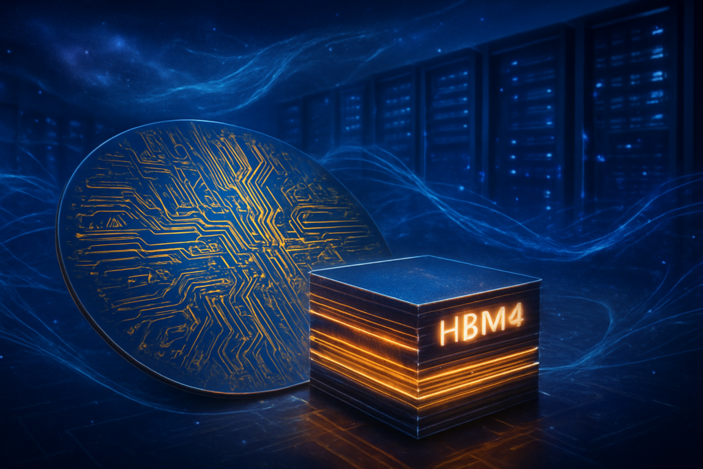
Breaking the Speed Limit: 11.7 Gb/s and the 2048-Bit Interface
The technical specifications of Samsung’s HBM4 are nothing short of revolutionary, pushing the boundaries of what was previously thought possible for DRAM performance. While the JEDEC Solid State Technology Association finalized HBM4 standards with a baseline data rate of 8.0 Gb/s, Samsung’s implementation shatters this benchmark, achieving a staggering 11.7 Gb/s per pin. This throughput is achieved through a massive 2048-bit interface—double the width of the 1024-bit interface used in the HBM3 and HBM3e generations—allowing a single HBM4 stack to provide approximately 3.0 TB/s of bandwidth.
Samsung is utilizing its most advanced 6th-generation 10nm-class (1c) DRAM process to manufacture these chips. A critical differentiator in this generation is the logic die—the "brain" at the bottom of the memory stack that manages data flow. Unlike its competitors, who often rely on third-party foundries like TSMC (NYSE: TSM), Samsung has leveraged its internal 4nm foundry process to create a custom logic die. This "all-in-one" vertical integration allows for a 40% improvement in energy efficiency compared to previous standards, a vital metric for data centers where NVIDIA’s Vera Rubin GPUs are expected to consume upwards of 1,000 watts per unit.
The initial reactions from the AI research community and industry experts have been overwhelmingly positive, albeit cautious regarding yield rates. Dr. Elena Kostic, a senior silicon analyst at SemiInsights, noted, "Samsung is essentially delivering 'overclocked' memory as a standard product. By hitting 11.7 Gb/s, they are providing NVIDIA with the headroom necessary to make the Vera Rubin platform a true generational leap in training speeds for Large Language Models (LLMs) and multi-modal AI."
A Strategic Power Play for the AI Supply Chain
The start of mass production in February 2026 places Samsung in a powerful strategic position. For NVIDIA, the partnership provides a diversified supply chain for its most critical component. While SK Hynix remains a primary supplier, the inclusion of Samsung’s ultra-high-speed HBM4 ensures that the Vera Rubin GPUs will not be throttled by memory bottlenecks. This competition is expected to exert downward pressure on HBM pricing, which has remained at a premium throughout 2024 and 2025 due to supply constraints.
For rivals like SK Hynix and Micron Technology (NASDAQ: MU), Samsung’s aggressive entry into the HBM4 market is a direct challenge to their recent market share gains. SK Hynix, which has dominated the HBM3e era with a nearly 60% market share, must now accelerate its own 1c-based HBM4 production to match Samsung’s 11.7 Gb/s performance. Micron, which had successfully captured a significant portion of the North American market, finds itself in a race to scale its capacity to meet the demands of the Vera Rubin era. Samsung’s ability to offer a "one-stop shop"—from DRAM manufacturing to advanced 2.5D packaging—gives it a lead-time advantage that could persuade other AI chipmakers, such as AMD (NASDAQ: AMD), to shift more of their orders to the Korean giant.
Scaling the Future: HBM4 in the Broader AI Landscape
The arrival of HBM4 marks a transition from "commodity" memory to "custom" memory. In the broader AI landscape, this shift is essential for the transition from generative AI to Agentic AI and Artificial General Intelligence (AGI). The massive bandwidth provided by HBM4 is required to keep pace with the exponential growth in model parameters, which are now frequently measured in the tens of trillions. Samsung’s development aligns with the industry trend of "memory-centric computing," where the proximity and speed of data access are more critical than raw compute cycles.
However, this breakthrough also brings concerns regarding the environmental footprint of AI. While Samsung’s HBM4 is 40% more efficient per gigabit, the sheer volume of memory being deployed in massive "AI factories" means that total energy consumption will continue to rise. Comparisons are already being drawn to the 2023 Blackwell launch; whereas Blackwell was a refinement of the Hopper architecture, Vera Rubin—powered by Samsung’s HBM4—is being described as a fundamental redesign of how data moves through an AI system.
The Road Ahead: 16-High Stacks and Hybrid Bonding
As mass production begins in February, the industry is already looking toward the next phase of HBM4 development. Samsung has indicated that while the initial production will focus on 12-high stacks, they are planning to introduce 16-high stacks later in 2026. These 16-high configurations will likely utilize "hybrid bonding" technology—a method of connecting chips without the use of traditional bumps—which will allow for even thinner profiles and better thermal management.
The near-term focus will be on the GTC 2026 conference in March, where NVIDIA is expected to officially unveil the Vera Rubin GPU. The success of this launch will depend heavily on Samsung's ability to maintain high yields during the February production ramp-up. Challenges remain, particularly in the complex assembly of 2048-bit interfaces, which require extreme precision in through-silicon via (TSV) technology. If Samsung can overcome these manufacturing hurdles, experts predict they could regain a 30% or higher share of the HBM market by the end of the year.
Conclusion: A New Chapter in the Semiconductor War
Samsung’s commencement of HBM4 mass production is more than just a product launch; it is a restoration of the competitive balance in the semiconductor industry. By delivering a product that exceeds JEDEC standards and integrating it into NVIDIA’s most advanced platform, Samsung has proven that it can still innovate at the bleeding edge. The 11.7 Gb/s data rate sets a new high-water mark for the industry, ensuring that the next generation of AI models will have the bandwidth they need to evolve.
In the coming weeks, the industry will be watching closely for the first shipments to NVIDIA’s assembly partners. The significance of this development in AI history cannot be overstated—HBM4 is the bridge to the next level of machine intelligence. As we move into February 2026, the "HBM War" has entered its most intense phase yet, with Samsung once again positioned as a central protagonist in the story of AI’s rapid advancement.
This content is intended for informational purposes only and represents analysis of current AI developments.
TokenRing AI delivers enterprise-grade solutions for multi-agent AI workflow orchestration, AI-powered development tools, and seamless remote collaboration platforms.
For more information, visit https://www.tokenring.ai/.